
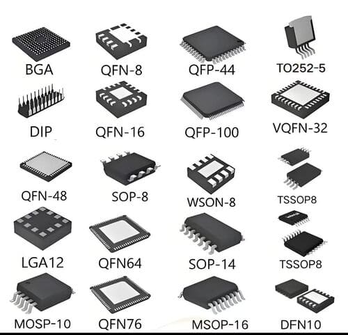
What does chip packaging look like?
What does chip packaging look like?
I. The Essence of Chip Packaging
Chip packaging (Package) serves three core functions, which are the fundamental design principles behind all package types.
First, it protects the internal bare die from moisture, oxidation, and mechanical damage during transportation and operation.
Second, it provides electrical interconnection, ensuring reliable connection between the internal circuitry of the chip and the PCB.
Finally, for high-performance or power devices, the package must also provide effective thermal dissipation to ensure long-term stable operation.
Because application scenarios vary, the emphasis on these three functions differs, leading to the development of various packaging structures.
II. Classification by Package Structure
After understanding the fundamental purpose of packaging, we can further categorize different package types by structural form. Generally, chip packages can be divided into four major categories: through-hole packages, surface-mount packages, high-density packages, and power device packages.
① Through-Hole Packages
This is one of the earliest and most intuitive package types. It is characterized by inserting pins into PCB holes for soldering, offering high mechanical reliability but larger size.
DIP (Dual In-line Package)
DIP is a classic dual in-line package with two rows of straight pins on both sides, resembling a “centipede-like” structure.
Due to its simple design, it is widely used in education, laboratory environments, and early electronic devices.
However, as electronics move toward miniaturization, DIP has gradually been replaced by surface-mount packages, though it is still used in prototyping and repair-friendly environments.
② Surface-Mount Packages (SMD / SMT Mainstream)
As PCB density increases, surface-mount technology has become mainstream. These packages are soldered directly onto the PCB surface, significantly saving space.
SOP / SOIC
SOP packages feature gull-wing leads on both sides, making them easy to manufacture and relatively easy to solder manually.
They are widely used in flash memory chips, power management ICs, and EEPROM devices.
Compared to DIP, SOP has become a standard in modern electronics, though it still has limitations in high-speed or high-density applications.
QFP (Quad Flat Package)
As chip functionality becomes more complex, single-side pin layouts are no longer sufficient, leading to the development of QFP packages.
QFP features pins on all four sides, significantly increasing the number of I/O connections.
It is commonly used in microcontrollers and industrial control chips, such as the STM32 series. However, due to its fine-pitch leads, it requires higher manufacturing and assembly precision.
QFN (Quad Flat No-lead)
When higher performance and smaller size are required, QFN becomes a better choice.
It eliminates exposed leads, with all electrical connections made through bottom pads, resulting in a smaller footprint and lower parasitic inductance.
Therefore, QFN is widely used in WiFi, Bluetooth, RF, and power management ICs.
However, since solder joints are not visible, it is more difficult to inspect and repair.
III. High-Density Packages (High-Performance Direction)
When chips evolve into CPU, GPU, or AI computing levels, the requirements for pin count and performance exceed the limits of traditional packages, leading to more advanced packaging technologies.
BGA (Ball Grid Array)
BGA transfers all electrical connections to the bottom of the chip in the form of a solder ball array.
This structure enables extremely high pin density within a very small area, making it the mainstream solution for high-performance chips.
Most CPUs, GPUs, and FPGAs use BGA packaging.
However, because solder joints are hidden, inspection and repair require specialized equipment such as X-ray systems.
CSP / WLCSP
For extreme miniaturization requirements, packaging can be reduced almost to the size of the bare chip itself, known as CSP or wafer-level chip scale packaging.
It is nearly equivalent to a “directly packaged bare die” and is extremely compact, making it ideal for smartphones and wearable devices.
However, it demands extremely high manufacturing precision and is very difficult to repair.
IV. Power Device Packages (Thermal Priority)
Unlike logic chips, power devices prioritize current handling and thermal performance, leading to a different set of packaging structures.
TO Package (TO-92 / TO-220)
TO packages typically include metal heat dissipation structures or larger pin designs, sometimes even with screw mounting holes.
This structure allows efficient heat transfer, making it ideal for MOSFETs, voltage regulators, and power amplifiers.
Although relatively large in size, it remains indispensable in high-power applications.
V. Package Type Comparison Summary
Overall, different packaging types represent trade-offs between size, performance, cost, and manufacturability.
| Type | Pin Structure | Characteristics | Typical Applications |
|---|---|---|---|
| DIP | Through-hole pins | Easy to repair, large size | Education, prototyping |
| SOP | Dual-side leads | Low cost, widely used | Flash, EEPROM |
| QFP | Four-side leads | High pin count | MCU, industrial control |
| QFN | Bottom pads | Compact, high performance | RF, wireless |
| BGA | Solder ball array | High density, high performance | CPU, GPU |
| CSP | Wafer-level | Ultra-miniature | Mobile chips |
| TO | Pins + heat sink | Power-oriented | MOSFET |