


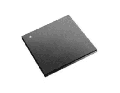
XCZU47DR-2FFVE1156I
AMD Xilinx Zynq UltraScale+ RFSoC
-
FPGA programmable logic
-
Integrated processing capabilities
-
RF signal conversion
-
Suitable for advanced communications and signal processing
We support Escrow payment and bank transfer (T/T). With Escrow, funds are held by a third-party platform and only released after you confirm receipt of the goods, ensuring transaction security.

Description
XCZU47DR-2FFVE1156I: Xilinx RFSoC FPGA
Product Overview
The XCZU47DR-2FFVE1156I belongs to the AMD Xilinx Zynq UltraScale+ RFSoC family, which brings programmable hardware, embedded processing, and RF signal-conversion capabilities together within one device.
In conventional RF systems, engineers may need to connect separate converters, processors, and programmable logic to handle incoming signals and generate processed outputs. An RFSoC-based design can consolidate some of these functions, helping reduce component interconnections and simplify hardware development.
The XCZU47DR is intended for demanding signal-processing architectures in which data acquisition, digital processing, and system control need to work together. Its suitability for a particular design depends on converter performance, processing requirements, interface configuration, and system-level constraints.
Key Technical Characteristics
- Manufacturer: AMD (Xilinx)
- Product family: Zynq UltraScale+ RFSoC
- Device number: XCZU47DR
- Device category: RFSoC with FPGA programmable logic
- Processing architecture: Embedded application and real-time processing
- RF conversion: Integrated analog-to-digital and digital-to-analog conversion resources
- Speed grade: -2
- Temperature grade: Industrial (I)
- Package designation: FFVE1156
- Package type: Flip-chip ball grid array (FCBGA)
The exact logic capacity, processor configuration, converter channel count, resolution, sampling rates, and electrical limits should be checked against the AMD documentation applicable to this specific device.
How the Device Works
The XCZU47DR combines several processing functions that can be coordinated within a single hardware platform.
RF signals can be converted into digital data through the integrated ADC resources. The programmable logic can then implement application-specific processing pipelines, while the embedded processing system manages software tasks, configuration, and system control. Integrated DAC resources can support the generation of analog signals from processed digital data.
This division of work allows designers to assign suitable tasks to dedicated hardware logic or embedded processors rather than relying on a general-purpose processor for every operation.
Depending on the design, this architecture can support:
- High-speed RF data acquisition
- Parallel digital signal processing
- Hardware acceleration for computationally demanding operations
- Embedded software and system management
- Digital signal generation and output conversion
- Coordinated control of processing and data-conversion functions
Actual functionality depends on the FPGA design, software, clocking, converter configuration, and external circuitry.
Package Information
The XCZU47DR-2FFVE1156I uses the FFVE1156 package designation.
- Package type: Flip-chip ball grid array (FCBGA)
- Mounting method: Surface-mount technology (SMT)
- Package-specific information: Refer to the manufacturer’s package documentation
Package dimensions, pin assignments, PCB land patterns, and assembly requirements should be obtained from the relevant AMD package files before beginning board design.
Electrical and Design Considerations
Integrating RF conversion and programmable processing into one device does not eliminate the need for careful hardware design.
Engineers should evaluate the following areas during system development:
- Power supply design and sequencing
- Reference clocks and clock distribution
- RF input and output signal integrity
- I/O voltage compatibility
- FPGA configuration and processor initialization
- PCB layout and thermal management
- Data throughput and processing latency
Power consumption and operating limits depend on the implemented design and operating conditions. Detailed voltage limits, timing requirements, and thermal specifications must be verified using the applicable AMD documentation.
Potential Applications
Wireless Communication
The combination of RF conversion and programmable processing can support wireless infrastructure designs that require configurable digital signal processing and high-speed data paths.
Radar and RF Systems
The integrated architecture can be considered for radar and other RF platforms that need to acquire, process, and generate signals within a coordinated hardware system.
Software-Defined Radio
Programmable logic and embedded processing can support flexible radio architectures in which signal-processing functions are implemented or adjusted through hardware logic and software.
Test and Measurement
RFSoC devices can be evaluated for equipment that requires integrated signal conversion and application-specific digital processing.
Aerospace and Defense Electronics
The architecture may suit selected signal-processing platforms where integration, processing performance, and configurable hardware are important. Final selection requires evaluation against the applicable technical and qualification requirements.
These are potential application areas, not a guarantee that the device meets every system’s performance or certification requirements.
Frequently Asked Questions
What is the XCZU47DR-2FFVE1156I?
It is an AMD Xilinx Zynq UltraScale+ RFSoC device that integrates programmable logic, embedded processing, and RF data-conversion capabilities.
What is the main design advantage of an RFSoC?
An RFSoC can combine functions that might otherwise require several separate devices. This may reduce interconnections and simplify system integration, depending on the application.
How does the programmable logic contribute to signal processing?
FPGA programmable logic allows engineers to implement application-specific parallel processing pipelines and hardware acceleration. The actual capabilities depend on the device resources and the implemented design.
Can the device be used in wireless communication or radar systems?
It can be evaluated for suitable wireless communication, radar, and other RF processing applications. Designers should compare the device’s verified specifications with their bandwidth, latency, converter, and processing requirements.
What should engineers verify before selecting this component?
Important considerations include the exact device variant, converter specifications, available logic resources, processor configuration, package pinout, electrical limits, thermal requirements, and lifecycle status.
Where can the official technical specifications be found?
Refer to AMD’s Zynq UltraScale+ RFSoC documentation and the applicable device and package documentation. These sources should take precedence over third-party summaries when designing hardware.
Explore more semiconductor industry information at Faith New Dawn.
Technical References
- AMD Zynq UltraScale+ RFSoC Product Data Sheet (DS889)
- AMD Zynq UltraScale+ RFSoC DC and AC Switching Characteristics (DS926)
- AMD Zynq UltraScale+ RFSoC Product Information
This content is an independently written product overview for identification and technical reference. Confirm device specifications with AMD documentation. Availability, condition, date code, and traceability should be verified separately.

Reviews
There are no reviews yet.